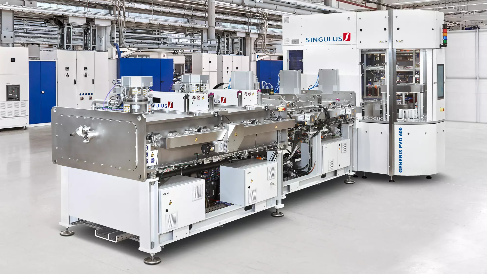
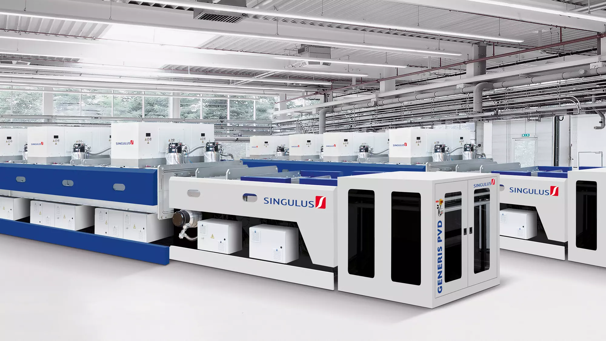
GENERIS PVD Inline Sputtering System
PVD/Sputtering Systems GENERIS PVD
Numerous SINGULUS TECHNOLOGIES vacuum sputtering machines are in operation in the solar industry, where SINGULUS TECHNOLOGIES provides the GENERIS PVD as a high throughput inline sputtering system platform with horizontal substrate transport. The GENERIS PVD ideally meets the key requirements of the heterojunction solar cell technology with respect to sophisticated transparent conductive oxide layers (TCO) such as ITO (Indium Tin Oxide) and AZO (Aluminum doped Zinc Oxide). The solar cells are automatically transported through the process chambers of the GENERIS PVD, following the inline principle, and applying coatings on both sides. The sputtering system safeguards a high level of layer thickness uniformity with high layer reproducibility, high productivity and at the same time very low operating expenses (OPEX).
With the latest system generation GENERIS PVD, SINGULUS TECHNOLOGIES can assure capacities up to 8,000 wafers per hour of G12 HJT cells. There are further savings due to the smaller footprint of the equipment and related smaller building and cleanroom space requirements. The dual-sided processes of the GENERIS PVD require less wafer handling resulting in reduced wafer breakage, wafer damage and wafer marks. SINGULUS TECHNOLOGIES takes advantage of in-house engineering of crucial components such as sputtering magnetrons, simulation and optimization of different sputtering processes and processes developed using state-of-the-art sputtering lab equipment at SINGULUS TECHNOLOGIES R&D center. Newly developed processes can be directly industrialized to the GENERIS PVD mass production platform.
Other PVD sputtering system with horizontal substrate transport: HISTARIS PVD
More about PVD sputtering system with vertical substrate transport: VISTARIS PVD
TYPICAL PERFORMANCE CHARACTERISTICS
- Sputtering materials: TCOs and other reactively sputtered layers: ITO, AZO, NiO, TiO2, SiN and more metallic layers: Ag, Cu, Cr, Mo, Ni and more
- Applications include anti-reflection layers, barrier layers, electrical contacting or insulating layers
- Available in different throughput versions of lab, pilot & mass production
- Wafer size: up to G12 & half cut formats
- Substrates thickness of down to 60 μm
- Typical tact time: 40 – 75 s per carrier
- Parallel processing of substrates (e.g. display, glass, Si wafers) via carrier tray
- High-speed automatization for carrier tray loading and unloading (single or double side)
- Top-down and bottom-up sputtering configurable – dual side sputtering without vacuum breakage
- Full substrate temperature control
- Low cost of ownership and high uptime
- Patented features such as fast venting systems and carrier
- Rotatable cylindrical magnetrons with highest utilization of target material
- Carrier return system (CRS) underneath
- Vacuum base pressure: ‹ 1 x 10⁻⁶ mbar


You have feedback or more questions?
Get in touch with us!
SINGULUS SALES TEAM
Phone: +49 6188 440-1292
Email: sales@singulus.de